A node.js-powered 8-bit CPU - part three
This post is part three of a series, the other posts available are
In part two we constructed a circuit using shift registers whereby we could write a byte of data and then read it back in. In this post we are going to look at a more complicated integrated circuit - a CPU - however the principles are the same.
In addition to the pieces required for the first two posts, you will need:
-
An additional bread board.
-
Enough LEDs and resistors for 16 more LEDs.
-
A 0.1µF “smoothing” capacitor.
-
An 8-bit CPU.
With that said, let’s meet my chosen CPU.
6809/6309
One of the advantages of retro computing is that we can easily (and reasonably cheaply) pick and choose anything we fancy, and so I’ve chosen the Hitachi 6309, specifically the HD63C09EP. This is Hitachi’s compatible version of the venerable 6809, which is considered by many to be the best 8-bit CPU ever made. Hitachi made it even faster and added some new instructions and registers, however it was developed right at the end of the 8-bit era, and with the introduction of 16-bit CPUs soon afterwards it didn’t have time to became as popular as its 8-bit counterparts such as the Z80, 6502 and 8008.
Thankfully, it’s still possible to buy them (second hand of course), and I managed to pick one up from littlediode.com for around £20.
To get started, let’s look at the pinout and describe what each pin does. Below is an ASCII diagram, with thanks to Jonathan Bowen’s 6809E manual (there are scanned PDFs of the original datasheets but the quality is not great).
                       _________    _________
                     _|         \__/         |_  ____
                Vss |_| 1                 40 |_| Halt  <--
                ___  _|                      |_
           -->  NMI |_| 2                 39 |_| TSC   <--
                ___  _|                      |_
           -->  IRQ |_| 3                 38 |_| LIC   -->
               ____  _|                      |_  _____
           --> FIRQ |_| 4                 37 |_| Reset <--
                     _|                      |_
           <--   BS |_| 5                 36 |_| AVMA  -->
                     _|                      |_
           <--   BA |_| 6                 35 |_| Q     <--
                     _|                      |_
                Vcc |_| 7                 34 |_| E     <--
                     _|                      |_
           <--   A0 |_| 8                 33 |_| Busy  -->
                     _|                      |_    _
           <--   A1 |_| 9                 32 |_| R/W   -->
                     _|                      |_
           <--   A2 |_| 10      6809E     31 |_| D0   <-->
                     _|                      |_
           <--   A3 |_| 11                30 |_| D1   <-->
                     _|                      |_
           <--   A4 |_| 12                29 |_| D2   <-->
                     _|                      |_
           <--   A5 |_| 13                28 |_| D3   <-->
                     _|                      |_
           <--   A6 |_| 14                27 |_| D4   <-->
                     _|                      |_
           <--   A7 |_| 15                26 |_| D5   <-->
                     _|                      |_
           <--   A8 |_| 16                25 |_| D6   <-->
                     _|                      |_
           <--   A9 |_| 17                24 |_| D7   <-->
                     _|                      |_
           <--  A10 |_| 18                23 |_| A15   -->
                     _|                      |_
           <--  A11 |_| 19                22 |_| A14   -->
                     _|                      |_
           <--  A12 |_| 20                21 |_| A13   -->
                      |______________________|
The arrows denote whether each pin is input, output, or both. Again, if a pin name has a line above it, for example Halt, it means it is “active low” and the function is activated when the pin is off/low, as opposed to being active when the pin is on/high.
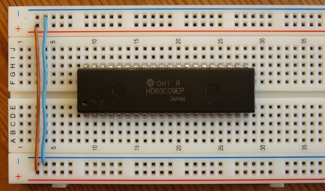
The CPU is placed onto the new bread board as shown below, so that the CPU straddles the middle of the breadboard, and the bottom side has more holes available - this helps with wiring as we will need more connections on that side.
We can sort the pins into logical groups, for now only concentrating on the bare minimum required to get things running.
Power (Vss/Pin1, Vcc/Pin7)
As with the shift registers, the CPU requires 5V to operate, and so we hook them up directly to the power rails. “Vss” is another term for ground.
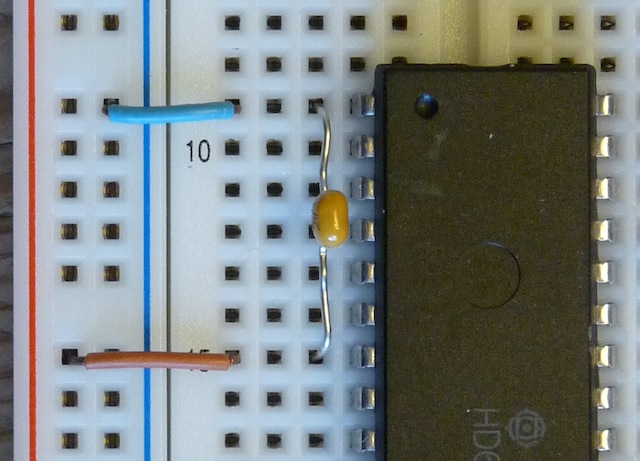
One recommended addition is an 0.1µF capacitor between Vss and Vcc. This acts like a small power buffer, and helps to smooth out any power fluctuations, ensuring that the CPU runs more reliably. Without this, you may notice odd behaviour, especially if you plug/unplug nearby electric devices.
To achieve maximum effectiveness, smoothing capacitors should be placed as close as possible to the input pins, as I’ve done in the picture below (again using brown/blue wires to denote power):
Clocks (E/Pin34, Q/Pin35)
Again, same deal as with the shift registers - the CPU needs a ticking clock in order to drive the internal circuitry. The 6309 has two clocks which must be driven in a specific order.
According to the datasheet “Q must lead E; that is, a transition on Q must be followed by a similar transition on E”. All that means is that repeating the following sequence is enough to drive the 6309 clock:
-
Set Q high
-
Set E high
-
Set Q low
-
Set E low
The speed at which we repeat this sequence determines the speed of the CPU. In the past with NMOS designs we would have had to keep running at a certain frequency for the chip to function correctly, but with newer CMOS designs we can run as slowly as we want, which is very helpful for seeing exactly what is happening.
By wiring E/Pin34 to GPIO17/Pin11 and Q/Pin35 to GPIO18/Pin12, we can run the CPU at 2Hz (two clock cycles per second) using a slightly extended version of our previous clock code:
var rpio = require('rpio');

rpio.setOutput(11);
rpio.setOutput(12);

/* 2Hz is slow enough to see what's happening without being overly cautious */
var speed = 2;

/*
 * Our repeating clock.  I've used the hour/quarter/half nomenclature as
 * a helpful visualisation of when each pin fires.  setInterval() and
 * setTimeout() take a millisecond argument, so we use parseInt() to ensure
 * no floating point.  This actually means we are limited to a clock speed
 * of 250Hz (one pin changing every millisecond) if we want a regular cycle.
 */
setInterval(function clock() {

	/* Set Q high immediately (on the hour) */
	rpio.write(12, 1);

	/* Set E high at quarter past the hour */
	setTimeout(function ehigh() {
		rpio.write(11, 1);
	}, parseInt(1000 / speed / 4 * 1));

	/* Set Q low at half past the hour */
	setTimeout(function qlow() {
		rpio.write(12, 0);
	}, parseInt(1000 / speed / 4 * 2));

	/* Set E low at quarter to the hour */
	setTimeout(function elow() {
		rpio.write(11, 0);
	}, parseInt(1000 / speed / 4 * 3));

}, parseInt(1000 / speed));
Data Bus (D0-7/Pin31-24)
With the 6309 being an 8-bit CPU, these are the 8 data pins on which a byte of data is read (“load”) or written (“store”) at a time. These are the only pins which are used for both input and output, and would normally be routed to a static RAM chip.
To get a CPU to do some work, we provide instructions (“opcodes”) and operands
(an address or a literal value) on the data bus. Let’s start with the simplest
program possible, a call to the nop (“No Operation”) instruction:
nop ; Do nothingWe can assemble this program using Ciaran Anscomb’s
asm6809.pl assembler and look at
the machine code it generated using od. This tells us the corresponding
opcode byte for the nop instruction:
: Assemble the source code in 6309-nop.s into an object file containing raw
: binary data.  No headers or object format data, just pure instructions.
$ asm6809.pl -o 6309-nop 6309-nop.s

: Display the contents of the binary in single-byte hexadecimal (-t x1) format.
$ od -t x1 6309-nop
0000000    12
0000001
So, to execute a nop instruction on the 6309, we write 0x12 onto the data
bus.
In the final post I will show how we can use our shift register setup to handle
the data bus, however for now we will simply hard-code a nop instruction on
the data bus, by wiring each bit either to the +5V or ground planes.
To calculate the pin settings for writing a particular byte, I wrote a small shell function to convert from hexadecimal to binary:
hex2bin8()
{
	printf "%08d\n" $(echo "16 i 2 o $(echo $1 | tr a-z A-Z) p" | dc);
}
which we can use like so:
$ hex2bin8 12
00010010
To execute a nop then, we set D1 and D4 to high and the rest to low (D0 is
the right-most bit, D7 is the left-most bit). Below is a picture of mine,
where I am using the green/white strands of the CAT5 cable for the data bus
connections.
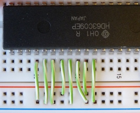
Due to the gaps on the power rails, we need to divert the D2 wire up a little to reach the ground rail, however it should hopefully be clear which rail each pin is connected to.
Address Bus (A0-A15/Pin8-23)
Whilst it is an 8-bit CPU, it has a 16-bit address bus, and so is able to directly address up to 65536 bytes of memory. The current address being read from or written to is output on these pins.
Again, these pins would normally be routed to some RAM chip, and by using the address in conjunction with the data bus, we can either load or store one byte of RAM at a time, with the address containing the particular area of memory to load or store, and the data containing the byte to be read or written.
For now, the most useful thing we can do is hook each of these pins up to an LED. By doing this we can simply show what address the CPU is currently at, even if it does mean converting from binary to hex.
Here is mine, using orange wire strips to denote the address bus:
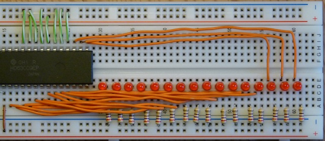
This can be a bit fiddly, due to the number of wires involved, but it should be possible to wire them all up as shown.
Note that the LEDs are back to front in terms of reading binary addresses. We could put them the other way around, but that would require a lot more cabling and it might get messy. This way we also match up the orientation of the data bus.
If you wanted to get fancy you could instead attach LED segment displays (or nixie tubes!), however I do not have any of those .. yet :)
Interrupts (NMI/Pin2, IRQ/Pin3, FIRQ/Pin4)
These pins allow you to send hardware interrupts which interrupt the CPU’s normal operation and execute specific functions. These would normally be used by something like an IO controller to indicate that, for example, some data has been read from disk and is now available.
For now we do not need any of these, so we simply disable these by hard wiring them to +5V (they are all active-low).
TSC/Pin39
This is the Tri-State Control pin, and can be used to synchronize data with other processors or controllers. As we do not have any of those yet, we simply hard wire it to GND and ensure this function is disabled.
Halt/Reset (Reset/Pin37, Halt/Pin40)
These pins are mostly self-explanatory, and are both active-low. This means that applying a negative voltage to Reset/Pin37 makes the CPU reset, and to Halt/Pin40 makes it pause indefinitely until Halt is released (set back to high).
For now we will keep things as simple as possible, and wire halt to +5V, effectively disabling it. We do however need to handle reset, as when the CPU is first powered on it needs a reset cycle to initialise correctly. This is done by holding reset down for at least one clock cycle, and so we will simply hook the reset pin to GPIO21/Pin13 and control this from software.
Alternatively, you could wire up a simple binary switch and have a hard reset button on your board.
Pin summary
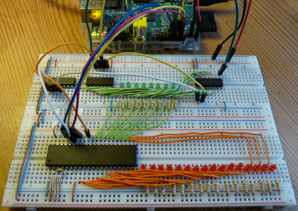
So, at this stage we should have the CPU wired up as following:
-
Power (Vss/Pin1 and Vcc/Pin7) wired to +5V and GND.
-
Clock E/Pin34 wired to GPIO17 (pin 11).
-
Clock Q/Pin35 wired to GPIO18 (pin 12).
-
Data bus (D0-D7/Pin31-24) wired to +5V/GND for
0x12(“nop”). -
Address bus (A0-A15/Pin8-23) wired to 16 LEDs.
-
Interrupts (NMI/Pin2, IRQ/Pin3, FIRQ/Pin4) wired to GND.
-
TSC/Pin39 wired to GND.
-
Reset/Pin37 wired to GPIO21 (pin 13).
-
Halt/Pin40 wired to +5V.
and the board should look something like this:
Software
We can extend our clock example above and add handling of the reset pin:
var rpio = require('rpio');

rpio.setOutput(11);
rpio.setOutput(12);
rpio.setOutput(13);

// Bump this to 2Hz from the clock example.
var speed = 2;

// Start with the reset pin held low while we start up the clock.
rpio.write(13, 0);

// The clock function is the same as before.
setInterval(function clock() {

	rpio.write(12, 1);

	setTimeout(function ehigh() {
		rpio.write(11, 1);
	}, parseInt(1000 / speed / 4 * 1));

	setTimeout(function qlow() {
		rpio.write(12, 0);
	}, parseInt(1000 / speed / 4 * 2));

	setTimeout(function elow() {
		rpio.write(11, 0);
	}, parseInt(1000 / speed / 4 * 3));

}, parseInt(1000 / speed));

/*
 * Ensure we run the clock at least once, then set the reset pin back high,
 * releasing the CPU to execute normally.
 */
setTimeout(function resethigh() {
	rpio.write(13, 1);
}, parseInt(2 * 1000 / speed));
Start It Up!
We now have everything in place to get the CPU running. Below is a video of mine, running at 2Hz.
At this point we can see and explain what happens right at the start of a CPU’s execution. I’ve trimmed the first second or so from the video where the CPU is running through its pre-initialisation routine. The video starts at the point where the CPU is reading the very first instructions from memory.
The 6309 starts by reading a byte each from 0xFFFE and 0xFFFF, and this
gives it the first 16-bit address to read from. You can see these first two
addresses shown by the LEDs at the beginning of the video. Remember that the
address LEDs are back-to-front, so the least-significant bit is on the left,
not the right.
Ordinarily there would be a ROM handling this part, and it would direct the CPU to start reading an area it has set aside to store a basic operating system. Once the address has been loaded, the CPU jumps to it and starts reading instructions.
As we are hard-coding the data bus with 0x12, the first address that the CPU
jumps to is 0x1212, shown by the 00010010 00010010 on the LEDs. At this
“address” the CPU again reads data from the data bus ready for its first
instruction, and of course gets another 0x12. This time it is executed as a
nop instruction, where the CPU does nothing for an instruction cycle.
This pattern then continues indefinitely:
-
The CPU increments the memory location where it should fetch the current instruction from. This is known as the “program counter” or “instruction pointer”.
-
The CPU reads an instruction from that location, in our case always reading
0x12which is its opcode for thenopinstruction. -
The
nopis executed, i.e. nothing happens.
Sure, it’s not practically useful. However, we are powering this entirely from JavaScript, we can see exactly what is happening, and for me at least it is immensely helpful having a visual overview of exactly how a CPU works.
The next and final step is to make the data bus controllable, so that we can issue arbitrary instructions and read back results. If only we had some way of reading and writing 8 bits of data using only a couple of GPIO pins… ;)
All Posts
- 16 Jul 2015 » Reducing RAM usage in pkgin
- 03 Mar 2015 » pkgsrc-2014Q4: LTS, signed packages, and more
- 06 Oct 2014 » Building packages at scale
- 04 Dec 2013 » A node.js-powered 8-bit CPU - part four
- 03 Dec 2013 » A node.js-powered 8-bit CPU - part three
- 02 Dec 2013 » A node.js-powered 8-bit CPU - part two
- 01 Dec 2013 » A node.js-powered 8-bit CPU - part one
- 21 Nov 2013 » MDB support for Go
- 30 Jul 2013 » What's new in pkgsrc-2013Q2
- 24 Jul 2013 » Distributed chrooted pkgsrc bulk builds
- 07 Jun 2013 » pkgsrc on SmartOS - creating new packages
- 15 Apr 2013 » What's new in pkgsrc-2013Q1
- 19 Mar 2013 » Installing SVR4 packages on SmartOS
- 27 Feb 2013 » SmartOS is Not GNU/Linux
- 18 Feb 2013 » SmartOS development preview dataset
- 17 Jan 2013 » pkgsrc on SmartOS - fixing broken builds
- 15 Jan 2013 » pkgsrc on SmartOS - zone creation and basic builds
- 10 Jan 2013 » Multi-architecture package support in SmartOS
- 09 Jan 2013 » Solaris portability - cfmakeraw()
- 08 Jan 2013 » Solaris portability - flock()
- 06 Jan 2013 » pkgsrc-2012Q4 illumos packages now available
- 23 Nov 2012 » SmartOS and the global zone
- 24 Oct 2012 » Setting up Samba on SmartOS
- 10 Oct 2012 » pkgsrc-2012Q3 packages for illumos
- 23 Aug 2012 » Creating local SmartOS packages
- 10 Jul 2012 » 7,000 binary packages for OSX Lion
- 09 Jul 2012 » 9,000 packages for SmartOS and illumos
- 07 May 2012 » Goodbye Oracle, Hello Joyent!
- 13 Apr 2012 » SmartOS global zone tweaks
- 12 Apr 2012 » Automated VirtualBox SmartOS installs
- 30 Mar 2012 » iptables script for Debian / Ubuntu
- 20 Feb 2012 » New site design
- 11 Jan 2012 » Set up anonymous FTP upload on Oracle Linux
- 09 Jan 2012 » Kickstart Oracle Linux in VirtualBox
- 09 Jan 2012 » Kickstart Oracle Linux from Ubuntu
- 22 Dec 2011 » Last day at MySQL
- 15 Dec 2011 » Installing OpenBSD with softraid
- 21 Sep 2011 » Create VirtualBox VM from the command line
- 14 Sep 2011 » Creating chroots for fun and MySQL testing
- 30 Jun 2011 » Graphing memory usage during an MTR run
- 29 Jun 2011 » Fix input box keybindings in Firefox
- 24 Jun 2011 » How to lose weight
- 23 Jun 2011 » How to fix stdio buffering
- 13 Jun 2011 » Serving multiple DNS search domains in IOS DHCP
- 13 Jun 2011 » Fix Firefox URL double click behaviour
- 20 Apr 2011 » SSH via HTTP proxy in OSX
- 09 Nov 2010 » How to build MySQL releases
- 29 Apr 2010 » 'apt-get' and 5,000 packages for Solaris10/x86
- 16 Sep 2009 » ZFS and NFS vs OSX
- 12 Sep 2009 » pkgsrc on Solaris
- 09 Dec 2008 » Jumpstart from OSX
- 31 Dec 2007 » Set up local caching DNS server on OSX 10.4