A node.js-powered 8-bit CPU - part two
This post is part two of a series, the other posts available are:
In part one we reached the stage where we were able to control an LED from node.js. We’re now going to move forward and control some simple Integrated Circuits (ICs). The principles are the same - using GPIO to turn pins on and off - but we use more pins to control something a bit more complicated.
The ICs we will look at in this post come from the 7400 series family of chips, which provide a whole variety of logic functions.
In addition to the pieces we needed for the introduction, you will need:
-
Enough LEDs and resistors for 8 lights.
-
Some wire for creating custom jumper lengths (I use CAT5 cable).
-
A 74HC595N and 74HC165N shift registers (the ‘N’ denotes that these are DIP and suitable for our bread board)
The shift registers can be bought very cheaply, most chips in the 7400 series cost less than a pound each.
Before we start, I prepare the breadboard like the picture below, where we configure both power rails with +5V (red jumper wire going to 5V/Pin2) and ground (black jumper wire going to GND/Pin6) to the Pi. The brown and blue wires come from a CAT5 cable, trimmed with wire cutters to fit, and are colour-coded to conform to IEC 60446.
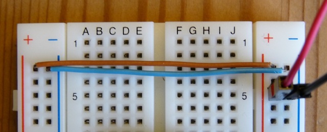
This allows us to easily bridge across to individual pins lower down the board.
I use CAT5 cable as it is a good size for the bread board, is strong enough to insert into the board yet flexible enough to be shaped to particular angles. It’s also really helpful that you get 8 different colour combinations to choose from, so that you can choose particular colours for specific functions, e.g. power, data, address, etc. However you could just use a lot of jumper wires if you prefer, they would certainly be quicker to set up.
Shift Registers
A shift register is an integrated circuit which is designed for serial-to-parallel or parallel-to-serial communication. Let’s dive straight in and take a look at an 8-bit serial-to-parallel shift register - the trusty 74HC595.
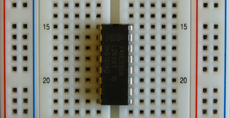
We start by placing the chip (be careful to avoid static electricity) onto the middle of the bread board. This allows us to connect to each pin, with the gap down the middle of the bread board used to separate each side.
Once we have done that, we need to look at the datasheet which explains the function of each of the pins. The full version is here but for now the only part we are concerned with is the pinout description:
By connecting to these pins and setting them high or low, we can control the function of this chip. Let’s go through them and describe what they do.
Power (Vcc/Pin16, GND/Pin8)
These pins provide the power that the chip requires to operate. Vcc is +5V and Vss is ground, so we can connect these directly to the corresponding power rails. I use the same colours (brown and blue) as above to make the functions of these pins clear.
For the connections to the Raspberry Pi, we use the ground pin as before, and now move our red wire over to Pin 2 which is +5V power.
So, to summarise:
-
Pin 2 on the RPi (+5V power) to one of the pins on either “+” (red line) power rail.
-
Pin 6 on the RPi (Ground) to one of the pins on either “-“ (blue line) power rail.
-
A small piece of brown wire connecting the nearest +5V rail to the line of Pin 16 (Vcc).
-
A small piece of blue wire connecting the nearest ground rail to the line of Pin 8 (GND).
This provides the power that the IC needs to function, now we need to start controlling its behaviour.
Serial Input/Output (DS/Pin14, Q7S/Pin9)
DS is the pin where we load our input, one bit at a time, by setting it either high or low. Q7S is the serial output pin, and is useful if you want to tie two 74HC595s together to form one 16-bit register, by taking the output of Q7S and feeding it to the DS input of the second 74HC595.
As we are only using one IC for now we can ignore Q7S. We want to input data though, so hook the DS pin to GPIO17, that is:
- Pin 11 on the RPi (GPIO17) to Pin 14 on the 74HC595 (DS).
We can leave the Q7S pin unconnected as it is used solely for output, though for your own experimentation you may want to hook it up and read the values while following the rest of this post.
Parallel Out (Q0-Q7/Pin15,1-7)
Once 8 bits of input have been loaded in, those 8 bits can then be output simultaneously on the parallel out pins. This gives us our serial-to-parallel conversion.
In order to show the output of these pins, we will hook them up to 8 LEDs. Start by laying out the LEDs on the board and insert a resistor for each, connecting between the ground rail and the cathode line, like so:
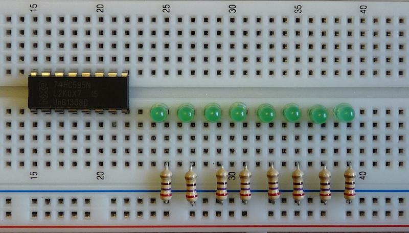
Next, cut and strip 8 lengths of wire and hook them up to their corresponding parallel output pin. In the picture below I have wired them up so that the LED furthest away is Q7 and the LED closest to the IC is Q0 (which is located on the other side, so the wire needs to go around the top of the IC).
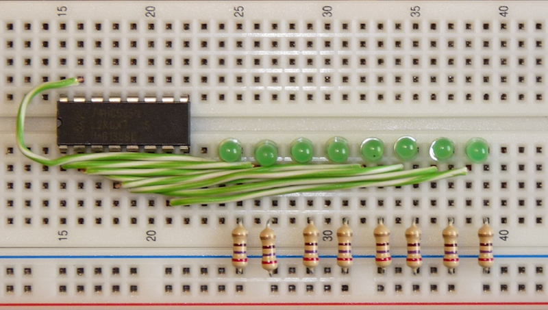
The reasons for doing it this way around will become clear later on, but for
now note that in this orientation it means that if we shift in e.g. 00001111,
the LEDs will show 11110000.
Clocks (SHCP/Pin11, STCP/Pin12)
Clocks are what get any integrated circuit running, with each tick/tock of a clock pin driving the internal circuitry. All that is required to generate a clock cycle is to switch a pin on and then off again. The speed at which a pin is cycled determines the speed at which the chip functions.
The 74HC595 contains two 8-bit storage registers, and each has its own independent clock for loading data. The diagram below is helpful for having a visual overview of how the chip is connected.
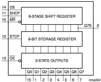
Data is read in from DS, using the SHCP clock to load one bit per clock cycle. After doing this 8 times, the data we want to load is now ready in the “8-stage shift register” shown above.
To load the 8-bits from the shift register into the storage register, a single clock cycle is required on the STCP clock. As soon as that happens, the data is latched into the “8-bit storage register”.
For simplicity, we will connect the two clock pins together, using a small piece of wire running vertically and joining the two lines. By doing this we can drive both clocks simultaneously from a single GPIO pin on the Raspberry Pi, which simplifies our software.
This means that on every clock cycle the data is copied from the shift register into the storage register, but this is helpful as it shows the data being loaded in.
To control the clocks from software, we wire either SHCP or STCP to pin 12 (GPIO18) on the Raspberry Pi.
Master Reset (MR/Pin10)
MR is useful if you just want to clear (set all to 0) the shift register, by
setting it low for one clock cycle, rather than shifting in 0 on the DS pin
for 8 clock cycles.
You’ll note the line above MR on the diagrams above. This denotes that this pin is “active low”, which means that its function is enabled when the pin is off, whereas all the other pins we have seen so far are “active high”, and they are active or enabled when on.
We don’t need to use this pin, so for now it is simply wired high (i.e. connected to the +5V power rail) and thus disabled.
Output Enable (OE/Pin13)
OE controls whether the data in the storage register is displayed on the parallel output. Again this is an “active low” pin, and for now we simply wire this low, to always enable output.
Wiring it all up.
At this point we have something which looks like this:
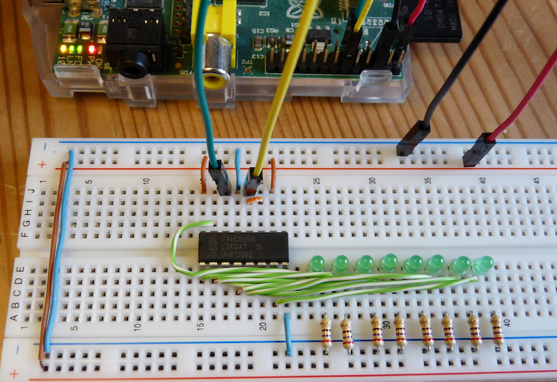
To summarise the various connections:
-
Power is provided to the bread board power rails from pin 2 (+5V) and pin 6 (GND) on the Pi.
-
Power is provided to the 74HC595 to pin 16 (Vcc, +5V) and pin 8 (GND) to the appropriate power rails using small strips of brown and blue wire.
-
DS is serial input and is wired using the green jumper wire to pin 11 (GPIO17) on the Pi.
-
STCP and SHCP are the clocks, and are joined together with a small piece of orange wire. One of them is then chosen (in my picture it is STCP) and connected using a yellow wire to GPIO18 (pin 12).
-
The parallel output pins (Q0-Q7) are hooked up to green LEDs using lengths of green wire.
-
The MR “master reset” pin 10 is hard wired to the +5V power rail to disable it (active low).
-
The OE “output enable” pin 13 is hard wired to the ground rail to enable it (active high).
The only pin which should be left unconnected is Q7S, unless you wish to hook it up to a spare GPIO pin on the Pi and verify what it is being set to at various points.
Software
We now write a small script to write some bits into the shift register. We start by setting up the two pins we want to control, and then we define an array which contains the bits we want to send into the chip.
One part which may be confusing is that we have one extra bit at the end of the input array. The reason for this is due to the clocks being linked together. According to the datasheet “If both clocks are connected together, the shift register will always be one clock pulse ahead of the storage register.” This means we need an extra clock cycle to update the storage register.
var rpio = require('rpio');

var pinDS = 11;
var pinClk = 12;

rpio.setOutput(pinDS);
rpio.setOutput(pinClk);

// Start with the clock pin low
rpio.write(pinClk, 0);

/*
 * This is what we want to send through the shift register - start with
 * all zeros to clear the buffer, then insert 10110111, with a final bit
 * to clock in the storage register.
 */
var input = [0, 0, 0, 0, 0, 0, 0, 0, 1, 0, 1, 1, 0, 1, 1, 1, 0];
For our clock function we will use something similar to the blinking LED example I showed in the first post, except this time on each “blink” we pop the first bit of input onto the DS pin. This loads the bit in, and we repeat until the input array is empty.
We can configure the clock speed with a variable - see the comment below.
/*
 * Configure the speed in Hz.  setInterval() and setTimeout have a maximum
 * resolution of 1ms, and we need a regular clock, so with each 'tick' and
 * 'tock' at a max of 1ms intervals our theoretical top speed is 500Hz.
 *
 * The 74HC595 is rated to 52MHz so we are in no danger of overclocking ;)
 */
var speed = 1;

setInterval(function clock() {

	/*
	 * Pop the first bit of input into DS.  If there is no more
	 * input then exit.
	 */
	if (input.length)
		rpio.write(pinDS, input.shift());
	else
		process.exit(0);

	/*
	 * Then cycle the clock at regular intervals, starting by setting it
	 * high then setting a timeout for half way until the next interval
	 * when we set it low.
	 */
        rpio.write(pinClk, 1);

        setTimeout(function clocklow() {
                rpio.write(pinClk, 0);
        }, parseInt(1000 / speed / 2));

}, parseInt(1000 / speed));
Ship It!
Running the program at 1Hz allows us to clearly see what happens, as shown in the video below. Prior to running the program and taking the video I set all the bits high, so that it is clear what happens when the first 8 zeros are shifted in.
That’s about it for the 74HC595, they are simple but incredibly useful devices.
And, as you might expect, there is a similar chip for doing parallel-to-serial conversion…
74HC165
The 74HC165 is an 8-bit parallel-to-serial IC, and pretty similar to the 74HC595. There are just a few differences we can note from the diagrams below:
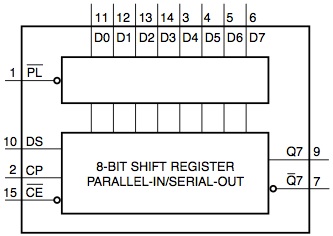
Unlike the 74HC595 there is no separate storage register, the data is loaded straight into the shift register and can then be read out.
We will hook it up to our bread board and use it to read the data from the 74HC595. Here is the pinout:
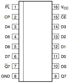
And the pins we are concerned with are:
-
Vcc/Pin16 and GND/Pin8 are our power pins, hook up the same as before.
-
D0-3/Pins11-14 and D4-7/Pins3-6 are the 8 parallel inputs. We connect D0 to the same LED that Q0 from the 74HC595 is output to, D1 to Q1 etc., all the way up to D7 to Q7.
-
PL/Pin1 is the active low “parallel load” pin, and when active reads 8-bits of data from the parallel input lines into the shift register. Afterwards, set it high and read out the data. We want to hook this up to pin 13 (GPIO21/27) on the Pi.
-
Q7/Pin9 is the serial output pin where we read data from, and we hook this up to pin 15 (GPIO22) on the Pi.
-
CP/Pin2 is the clock for reading data out. CE/Pin15 is an active low clock enable. As we can use the PL pin to control when to load the parallel input, we do not need a separate clock for this chip and can simply link it to the 74HC595 clock with a jumper wire.
DS/Pin10 and Q7/Pin7 are serial input/output pins, and can be useful for daisy-chaining, however we have no need for them, and can leave them unconnected.
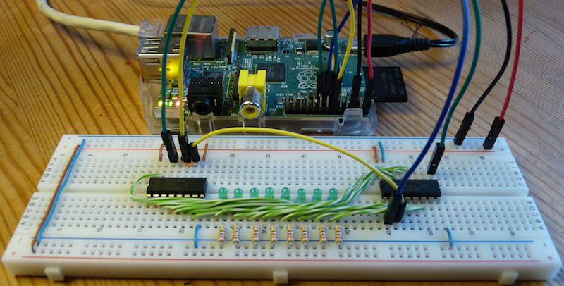
After performing all of the connections above, it should look something like this:
As for software, the program below takes a single argument of a byte of data, loads it into the 74HC595, then reads it out from our data bus using the 74HC165 before displaying the two for comparison. If everything went well, the two bytes should be identical.
var rpio = require('rpio');

/*
 * The byte we will write and hopefully read back.
 */
var outbyte = parseInt(process.argv[2], 16);

/*
 * Set up our pin mappings and configure them.
 */
var pin = {
	'output': 11,
	'clock': 12,
	'pload': 13,
	'input': 15,
}

rpio.setOutput(pin.output);
rpio.setOutput(pin.clock);
rpio.setOutput(pin.pload);
rpio.setInput(pin.input);

/*
 * The clock and parallel read pins are triggered on a transition
 * to high, so we start with them low.
 */
rpio.write(pin.clock, 0);
rpio.write(pin.pload, 0);

/*
 * Function to cycle (high then low) a specified pin.
 */
var cycle = function (p)
{
	rpio.write(p, 1);
	rpio.write(p, 0);
}

/*
 * Ensure that our output is converted to binary and is padded.
 */
outbyte = String("00000000" + outbyte.toString(2)).slice(-8);

/*
 * Shift the output onto the 'DS' pin one bit at a time followed by
 * a clock to load it into the shift register.
 */
outbyte.split('').forEach(function (bit) {
	rpio.write(pin.output, bit);
	cycle(pin.clock);
});

/*
 * If the shift and storage clocks are connected, as they are in our setup,
 * then the storage clock will always trail the shift clock by one pulse, so
 * we need to do one final cycle to syncronise it with our input.
 *
 * We can then cycle the parallel load pin to clock the data into the 74HC165.
 */
cycle(pin.clock);
cycle(pin.pload);

/*
 * Finally, read in the data from the 74HC165, one bit at a time.  As we have
 * read the data from the 74HC595 we can ignore the fact that these clock
 * cycles will now "corrupt" the 74HC595's storage with whatever the last bit
 * we set pin.output to.
 */
var inbyte = "";
for (var i = 0; i < 8; i++) {
	inbyte += rpio.read(pin.input);
	cycle(pin.clock);
}

/*
 * Convert both bytes to hexadecimal and print our final sanity check.
 */
outbyte = parseInt(outbyte, 2);
console.log("send: 0x%s", String("00" + outbyte.toString(16)).slice(-2));

inbyte = parseInt(inbyte, 2);
console.log("recv: 0x%s", String("00" + inbyte.toString(16)).slice(-2));
The output should look like this:
# node shifty.js 0xb7
send: 0xb7
recv: 0xb7
Congratulations! You have added 8 bits of storage to your computer! ;)
As you may appreciate, the 7400 series of chips can be incredibly useful, somewhat like lego where you can use them for building blocks into larger things. One engineer has even used them exclusively to build an entire computer - including creating a custom CPU!
I’m not quite that adventurous, so in the next post I will use an existing CPU and show how we can drive it in a similar way to the shift registers above.
All Posts
- 16 Jul 2015 » Reducing RAM usage in pkgin
- 03 Mar 2015 » pkgsrc-2014Q4: LTS, signed packages, and more
- 06 Oct 2014 » Building packages at scale
- 04 Dec 2013 » A node.js-powered 8-bit CPU - part four
- 03 Dec 2013 » A node.js-powered 8-bit CPU - part three
- 02 Dec 2013 » A node.js-powered 8-bit CPU - part two
- 01 Dec 2013 » A node.js-powered 8-bit CPU - part one
- 21 Nov 2013 » MDB support for Go
- 30 Jul 2013 » What's new in pkgsrc-2013Q2
- 24 Jul 2013 » Distributed chrooted pkgsrc bulk builds
- 07 Jun 2013 » pkgsrc on SmartOS - creating new packages
- 15 Apr 2013 » What's new in pkgsrc-2013Q1
- 19 Mar 2013 » Installing SVR4 packages on SmartOS
- 27 Feb 2013 » SmartOS is Not GNU/Linux
- 18 Feb 2013 » SmartOS development preview dataset
- 17 Jan 2013 » pkgsrc on SmartOS - fixing broken builds
- 15 Jan 2013 » pkgsrc on SmartOS - zone creation and basic builds
- 10 Jan 2013 » Multi-architecture package support in SmartOS
- 09 Jan 2013 » Solaris portability - cfmakeraw()
- 08 Jan 2013 » Solaris portability - flock()
- 06 Jan 2013 » pkgsrc-2012Q4 illumos packages now available
- 23 Nov 2012 » SmartOS and the global zone
- 24 Oct 2012 » Setting up Samba on SmartOS
- 10 Oct 2012 » pkgsrc-2012Q3 packages for illumos
- 23 Aug 2012 » Creating local SmartOS packages
- 10 Jul 2012 » 7,000 binary packages for OSX Lion
- 09 Jul 2012 » 9,000 packages for SmartOS and illumos
- 07 May 2012 » Goodbye Oracle, Hello Joyent!
- 13 Apr 2012 » SmartOS global zone tweaks
- 12 Apr 2012 » Automated VirtualBox SmartOS installs
- 30 Mar 2012 » iptables script for Debian / Ubuntu
- 20 Feb 2012 » New site design
- 11 Jan 2012 » Set up anonymous FTP upload on Oracle Linux
- 09 Jan 2012 » Kickstart Oracle Linux in VirtualBox
- 09 Jan 2012 » Kickstart Oracle Linux from Ubuntu
- 22 Dec 2011 » Last day at MySQL
- 15 Dec 2011 » Installing OpenBSD with softraid
- 21 Sep 2011 » Create VirtualBox VM from the command line
- 14 Sep 2011 » Creating chroots for fun and MySQL testing
- 30 Jun 2011 » Graphing memory usage during an MTR run
- 29 Jun 2011 » Fix input box keybindings in Firefox
- 24 Jun 2011 » How to lose weight
- 23 Jun 2011 » How to fix stdio buffering
- 13 Jun 2011 » Serving multiple DNS search domains in IOS DHCP
- 13 Jun 2011 » Fix Firefox URL double click behaviour
- 20 Apr 2011 » SSH via HTTP proxy in OSX
- 09 Nov 2010 » How to build MySQL releases
- 29 Apr 2010 » 'apt-get' and 5,000 packages for Solaris10/x86
- 16 Sep 2009 » ZFS and NFS vs OSX
- 12 Sep 2009 » pkgsrc on Solaris
- 09 Dec 2008 » Jumpstart from OSX
- 31 Dec 2007 » Set up local caching DNS server on OSX 10.4